- 您现在的位置:买卖IC网 > Sheet目录1994 > DS3105LN+ (Maxim Integrated Products)IC TIMING LINE CARD 64-LQFP
DS3105
25
7.7
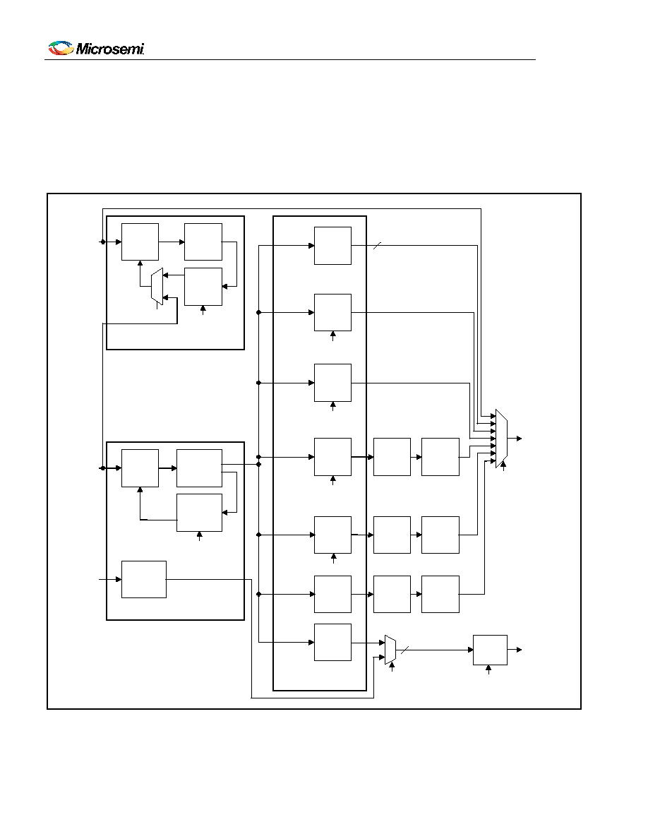
DPLL Architecture and Configuration
Both the T0 DPLL and T4 DPLL are digital PLLs. The T0 DPLL has separate analog PLLs (APLLs) as output
stages as well as some outputs that are not cleaned up by an APLL. This architecture combines the benefits of
both PLL types. See Figure 7-1.
Figure 7-1. DPLL Block Diagram
T0 DPLL
T4 DPLL
Locking
Frequency
T0
PFD and
Loop Filter
T0
Foward
DFS
T0
Feedback
DFS
DIG12
DFS
T0 selected
reference
OC3, OC6
T4
Foward
DFS
T4
Feedback
DFS
T4
PFD and
Loop Filter
Locking
Frequency
T4 selected
reference
T0CR1:T0FREQ[2:0]
OCRm:OFREQn[3:0]
OCR5:AOFn
T0CR1:T4MT0
T4CR1:T4FREQ[3:0]
T0CR1:T0FT4[2:0]
1
0
APLL
Output
Dividers
T0
Output
APLL
T0
APLL
DFS
APLL
Output
Dividers
T4
Output
APLL
T4
APLL
DFS
DIG12
DFS
2K8K
DFS
MCR6:DIG2SS
MCR6:DIG2F[1:0]
MCR6:DIG2AF
MCR6:DIG1SS
MCR6:DIG1F[1:0]
OUTPUT DFS
FSYNC
DFS
SYNC2K
FSCR2:INDEP
DIG2
DIG1
2K8K
ICRn:FREQ[3:0]
APLL
Output
Dividers
T0
Output
APLL2
T0
APLL2
DFS
2
FSYNC,
MFSYNC
OCR4:FSEN, MFSEN
FSCR1:8KINV, 2KINV
FSCR1:8KPOL, 2KPOL
PLL Bypass
发布紧急采购,3分钟左右您将得到回复。
相关PDF资料
DS3106LN+
IC TIMING LINE CARD 64-LQFP
DS3231MZ+
IC RTC I2C 8SOIC
DS3231SN#T&R
IC RTC W/TCXO 16-SOIC
DS3232MZ+
IC RTC W/SRAM I2C 8SOIC
DS3232SN#T&R
IC RTC W/TCXO 20-SOIC
DS3234S#
IC RTC W/TCXO 20-SOIC
DS32C35-33#T&R
IC RTC ACCURATE I2C 3.3V 20-SOIC
DS3911T+
IC DAC 10BIT I2C QUAD 14TDFN
相关代理商/技术参数
DS3106
制造商:MAXIM 制造商全称:Maxim Integrated Products 功能描述:Line Card Timing IC
DS3106A10SL3S(621)
制造商:Amphenol Corporation 功能描述:
DS3106A14S2S
制造商:Amphenol Corporation 功能描述:
DS3106A14S2S(621)
制造商:Amphenol Corporation 功能描述:
DS3106A14S5P
制造商:Amphenol Corporation 功能描述:
DS3106A14S5P(621)
制造商:Amphenol Corporation 功能描述:
DS3106A14S5S(621)
制造商:Amphenol Corporation 功能描述:
DS3106A14S6P
制造商:Amphenol Corporation 功能描述: